
Help
Why you need a lab assistant when you breadboard
Wiring your first physical breadboard is a frustrating experience. One wrong connection and the circuit does not work. Without an experienced lab or teaching assistant by your side, it is difficult to find out where is the mistake. Our breadboard simulator acts as a virtual and patient lab assistant who checks your every connection to help you gain experience and confidence to breadboard correctly.
Practice does not make perfect. Only perfect practice makes perfect - Vince Lombardi
verified_user Complete wiring one circuit in this breadboard simulator and earn a digital badge. You need to sign in with your Google account first.
To complete wiring the breadboard
- Operate the switches in the circuit simulator. Read the description of the circuit for more information. The default circuit is the 1 to 2 demultiplexer. It is an easy circuit to understand and to breadboard.
- Using the circuit schematic, wire up the circuit in the breadboard simulator. When a wire end is placed in a socket of the breadboard that corresponds to a node on the schematic, the respective node of the schematic will turn red.
- If a correct connection is made, the wire ends will snap into the socket.
- When all the nodes are wired up, a red LED will light up near the VCC/GND terminals to indicate that the breadboard wiring is completed correctly.
- You may now operate the switches of the breadboard and observe the LED results.
Notes
- Click Help on menu to hide/show this Help panel. This site is optimised for computer browsers.
- All the VCC (red wire) and GND (black wire) connections are already done. When you wire up the actual circuit using the low cost Home Laboratory Kit, do remember to connect the VCC and GND wires.
- When you select a different schematic, the ones where you have completed the breadboard will be shown with a green background.
- The holes in the breadboard connected in blue are electrically connected.
- If you are unfamiliar with the breadboard, there are many resources available online that explains how they work. We recommend this quick Breadboard Infographic from Make Breadboarding Workshop or the longer Breadboard Tutorial from Science Buddies.
- Read Stony Brook University's paper that reports how their "virtual breadboard helped students to prepare for their labs, and significantly reduced the amount of time teaching assistants had to spend helping students in the actual lab."
Breadboard Simulator
Circuit Schematic & Simulator
SR NAND latch
When using static gates as building blocks, the most fundamental latch is the simple SR latch, where S and R stand for set and reset. It can be constructed from a pair of cross-coupled NOR or NAND logic gates. The stored bit is present on the output marked Q.
The circuit is a basic NAND latch. The inputs are generally designated S and R for Set and Reset respectively. Because the NAND inputs must normally be logic 1 to avoid affecting the latching action, the inputs are considered to be inverted in this circuit (or active low).
The circuit uses feedback to "remember" and retain its logical state even after the controlling input signals have changed. When the S and R inputs are both high, feedback maintains the Q outputs to the previous state.
The R = S = 0 combination is called a restricted combination or a forbidden state because, as both NAND gates then output 1s, it breaks the logical equation Q = not Q. The combination is also inappropriate in circuits where both inputs may go high simultaneously (i.e. a transition from restricted to keep). The output would lock at either 1 or 0 depending on the propagation time relations between the gates (a race condition). In certain implementations, it could also lead to longer ringings (damped oscillations) before the output settles, and thereby result in undetermined values
-
Notes:
- Q0 is the previous state of Q and Q0 is the previous state of Q.
- R and S are asynchronous inputs - that is the output responds to these input immediately. They are active low inputs. Click on their respective switches (SW6 and SW7) and observe.
- S sets the output to 1 and R resets the output to 0.
- Both R and S cannot be low at the same time - the output is undefined.
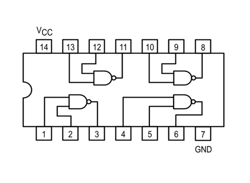
7400 NAND Gate IC Pin Out